


Information source: China Electric Power
The thermal characteristics and thermal design of IGBT module are summarized. The thermal impedance network model of IGBT module and its relationship with the thermal properties and size of packaging materials are introduced. The key points of thermal design of the module are discussed from the aspects of packaging materials and structure of the chip and module, and the thermal design of the traditional IGBT module and the new crimped IGBT module is described.
Keywords: semiconductor; IGBT module; Thermal design; Reliability; Thermal solutions
Foreword
High-power semiconductor devices are the units that realize energy generation, transmission, conversion and control. They are the core components of power electronics systems, and they determine the performance, efficiency, reliability, cost, volume and weight of power systems to a large extent. At present, in the field of high power semiconductor devices of 600 V and above, the main products are the insulated gate bipolar transistor (IGBT) and the corresponding freewheeling diode (FWD). The basic unit of the power semiconductor device is the chip. Based on the yield, consistency and manufacturability, the size of IGBT chip is generally less than 200 mm2, and the maximum current can reach about 300 A. In order to meet the requirements of high-power system, IGBT and FWD chips are generally packaged in parallel into IGBT module structure. IGBT module not only realizes the electrical interconnection between chips, the connection of the moving unit and the external main circuit, but also plays the role of support, protection, heat dissipation and so on.
As an application unit of high-power semiconductor devices, the package form, structure, technology and materials of IGBT module largely determine the overall performance and reliability of the module. Therefore, the packaging technology of IGBT module is of vital significance to the industry and users. The design, manufacturing, testing and reliability of IGBT module has always been one of the key issues in the research and development of power semiconductor.
IGBT and other power semiconductor devices are not ideal switching components, in the on-state, the chip itself has a certain resistance, resulting in on-state loss; In the switching process, due to the time delay, the voltage and current overlap, resulting in switching loss. The power loss causes the chip junction temperature (Tj) to rise, and thermal failure will occur when the maximum allowable junction temperature (Tjmax) is exceeded. Therefore, the heat generated by the loss must be quickly and efficiently emitted to reduce the high Tj damage to the chip and improve the reliability and life of the chip.
The thermal design of IGBT module is to reduce the thermal resistance (Rth j-c) and thermal time constant (τ) from the chip to the shell (substrate) through the design of structure, material and packaging technology, so as to realize the fast and efficient heat emitted by the device to the shell. In addition, in practical applications, the heat flow reaching the module housing needs to be effectively dissipated to the external radiator or cooling system through the thermal management techniques of the system.
This paper mainly summarizes the thermal behavior and thermal design of traditional IGBT module and the thermal design method of new crimped IGBT module. The relationship between the thermal resistance and the thermal performance and size of packaging materials is discussed by the IGBT thermal impedance network model. The influence of power loss on junction temperature and temperature change on module life of power semiconductor devices is discussed. The key points of thermal design of the module are analyzed from the aspects of the package structure and materials of the chip and module, and the thermal management scheme of IGBT module in the application system is also analyzed.
1 Thermal resistance network of the IGBT module
The structural profile of the traditional IGBT module is shown in Figure 1. The ceramic lining board is used to realize the insulation between the chip and the outside, and the substrate plays the role of heat dissipation, support and contact with the external heat sink. Electrical interconnection and connection are realized through aluminum lead bonding and solder layer.
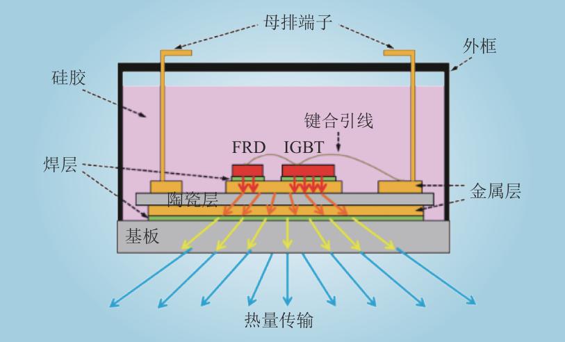
Figure 1. Traditional IGBT module structure profile
The bonding point between the aluminum bonding lead of the module and the chip is small, and the heat generated during the working of the chip is mainly transferred from the chip to the substrate through the way of heat conduction. In this process, certain resistance will be encountered, which is called thermal conductivity resistance. The thermal resistance Rth j-c from chip to shell is the sum in series of the thermal resistance of each layer of materials along the heat dissipation path. According to Formula (1), the thermal resistance and heat capacity of each layer of material are determined by its heat dissipation area and thickness, and the heat dissipation area is determined by the thermal diffusion Angle α of the material.
Where: Rth is the thermal conductivity resistance of the material; d is the thickness of thermal conductivity medium layer; k is thermal conductivity; A is the area of heat conduction medium; C is the heat capacity; c is the specific heat capacity of the material; m is the material mass. In the heat dissipation path of IGBT module, from the chip down, the heat dissipation area A gradually increases. Assuming that the heat dissipation Angle α is constant and the heat conduction area is square, as shown in Figure 2, then the heat conduction medium area Ai of the i layer is approximately estimated by Equation (2).

Where, di is the thickness of the I-th layer; li−1 is the side length of the i-1 layer thermal conductivity medium.

Figure 2. Heat dissipation area of different media in the heat dissipation path of IGBT module
According to the Cauer model, the equivalent thermal resistance network of the traditional IGBT module is shown in Figure 3. Based on the actual physical significance, the overall thermal resistance is equivalent to the sum of the thermal resistance of each layer of thermal conductivity medium, and the heat capacity of each medium is determined by its material properties and quality. According to this model, the Rth j-c of IGBT module can be calculated.
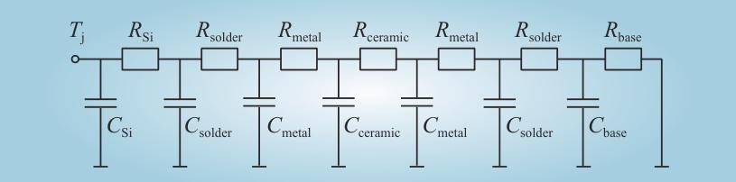
Figure 3 Cauer model of equivalent thermal resistance network of IGBT module
2 Thermal design and thermal management of IGBT module
The Rth j-c of IGBT module is directly related to the chip area. The larger the chip area is, the larger the cross-sectional area of the heat dissipation channel is, and the smaller Rth j-c is. However, in order to improve the power density of the module and power system and reduce the volume, the current research and development focus is to gradually increase the current density of the chip and reduce the overall area of the chip, thus increasing the Rth j-c. The chip power consumption and Rth j-c can be reduced to a certain extent by using wafer technology. In the design of IGBT module, it is necessary to reduce the increase of thermal resistance caused by high power density chip by optimizing the structure and material. By increasing the Tjmax of the chip, the thermal design margin and module reliability are increased.
2.1 Influence of packaging materials on thermal characteristics
In addition to semiconductor chips, the packaging materials of traditional IGBT module mainly include insulation lining board, busbar terminal, bonding lead, solder, substrate, silica gel, plastic shell, etc. The key of material thermal design is to select the material combination with high thermal conductivity and high CTE matching rate, so as to reduce the thermal resistance and reduce the thermo-mechanical stress. Thermal mechanical stress is the main cause of thermal fatigue degradation and failure of power modules. It is caused by different CTE of materials in the process of temperature change, and has the greatest influence on the bonding layer and interconnect part of the module. Therefore, optimizing the selection of module materials based on thermal characteristics is an important step to improve the thermal stability and life of modules.
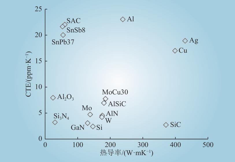
Figure 4. Thermal characteristics of commonly used packaging materials for IGBT module
Figure 4 shows the main thermal parameters of commonly used packaging materials for IGBT module. At present, the commonly used insulating lining board mainly includes Al2O3, AlN, Si3N4, etc. In terms of thermal characteristics, AlN is the ideal packaging material, and also the primary choice of most IGBT modules. However, Al2O3 has the advantage of cost, Si3N4 has the advantage of mechanical strength, which needs to be considered in the design according to the application requirements. IGBT module commonly used chip interconnect material is Al bond lead, but its thermal and electrical conductivity are weaker than Cu material, and CTE is larger than Cu, in the temperature shock, the heat-mechanical stress is greater, the reliability is lower. Therefore, copper wire bonding has the advantages of electricity, thermal, reliability and so on. It is the development trend of power module packaging materials and technology.
At present, the substrate materials of IGBT module mainly include Cu, AlSiC and Cu alloy. Cu material has high thermal conductivity, but CTE is very different from Si, lining and other materials, which is easy to produce large thermal mechanical stress in the work. AlSiC has higher CTE matching degree and higher thermal conductivity with other materials in the module system, so it is often chosen as the packaging material for high-reliability modules.
For potting materials such as silica gel and shell, the operating temperature range and thermal stability are the key parameters to be considered, which are generally tested through high and low temperature storage and impact tests. Especially for power modules applied under harsh temperature conditions, temperature characteristics and stability are important assessment indicators of module potting materials.
2.2 Thermal design scheme of module structure
The structure of IGBT module determines its thermal resistance to some extent. Figure 3 shows the equivalent thermal resistance network based on the traditional IGBT module structure, indicating that Rth j-c is determined by the heat dissipation path of the module structure. In applications, the heat transmitted to the module housing will be taken away by the external radiator, so the thermal resistance Rth c-h from the module to the radiator is an important part of the module thermal design and thermal management. The thermal resistance Rth j-h from the chip to the external radiator can be expressed as

In application, about 0.1mm thick thermal grease is applied between the flat base plate housing and the heat sink of the traditional module to fill the gap between the base plate and the heat sink and increase the heat dissipation efficiency. Due to the low thermal conductivity of thermal grease, generally Rth c-h accounts for about 50% of the overall thermal resistance Rth j-h. Through the module packaging structure design, such as direct heat dissipation, the thermal grease layer can be removed in the application, greatly reducing the overall thermal resistance.
2.2.1 Direct water cooling heat dissipation structure
Figure 5 shows the structure diagram of direct liquid Cooling (DLC) IGBT module. The Pin Fin substrate is adopted to realize direct liquid cooling without thermal grease layer and external heat sink. Compared with the traditional flat substrate structure, the Rth j-h is reduced by about half, as shown in Figure 6.
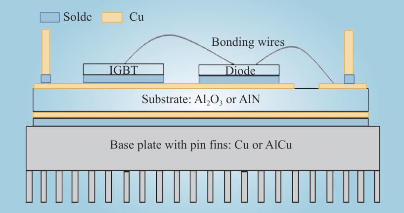
Figure 5 DLC IGBT module structure
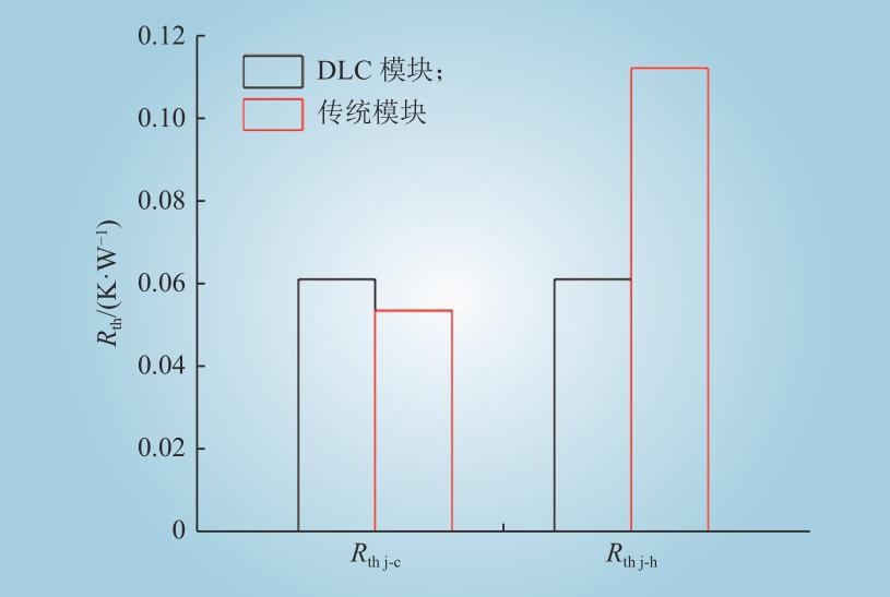
FIG. 6 Comparison of thermal resistance between DLC and traditional IGBT module
2.2.2 Double-sided heat dissipation structure of flat package
The planar packaging structure uses metal layer to replace the aluminum bonding lead interconnection on the chip surface, which can reduce the electrical parasitic parameters, improve the current carrying capacity, and has a series of advantages in electrical, thermal, mechanical and reliability.
Through planar packaging structure and technology, heat loss generated by IGBT modules can be spread through both upper and lower radiators to achieve double sided cooling (DSC). The calculation formula of the crust equivalent thermal resistance of Rth j-c DSC structure is shown in Equation (4), where Rth j-c T and Rth j-c B are the thermal resistance of the chip to the upper and lower surface of the shell respectively. The symmetrical design can double the heat dissipation efficiency of the module and reduce the equivalent Rth j-c by about half, thus greatly reducing Tj and improving the thermal performance and temperature reliability.

FIG. 7 is the structure diagram of the newly developed DSC plane package automotive IGBT module developed by Zhuzhou CRRC Time Electric. The power chip is connected to two layers of insulating liner by welding or silver sintering technology, and the current channel passes through the copper coating of the upper liner. The heat generated by the chip is diffused through the two liners to the external radiator. The module shell is formed by rotary die technology, which has high working temperature and reliability.
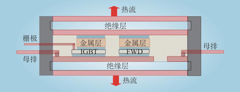
FIG. 7 Structure of planar package DSC IGBT module
DSC module has no substrate, its Rth j-h is more than 50% lower than that of DLC module. However, since there is no integrated direct water-cooled radiator, the application requires contact with the external radiator through thermal conductivity material or welding, thus increasing the Rth j-h. Figure 8 shows the equivalent Rth j-h of DSC module in different installation modes and the comparison between DSC module and DLC module. Compared with DLC module, the Rth j-h of DSC module is reduced by 30%. This value is affected by the thermal conductivity of DSC module. The Rth j-h of DSC module installed by welding is about 40% less than that of DLC structure.
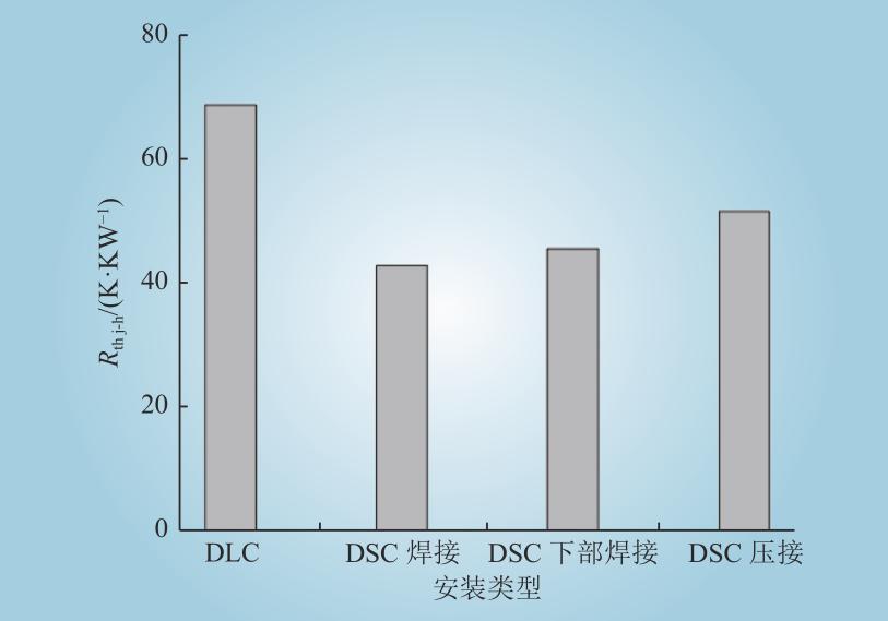
FIG. 8 DSC module Rth j-h and its comparison with DLC module
2.2.3 Integrated phase change structure cooling structure
Heat absorption by changing the physical state of a phase change material, such as the evaporation of a liquid into a gas. Heat pipe or steam chamber is a structure that realizes heat dissipation by the liquid phase transition process. It has high heat dissipation efficiency and has been applied in the thermal management of power semiconductor devices and systems. However, the structure is generally used as an external heat dissipation design, which is applied outside the power module. When the heat pipe or steam chamber structure is integrated into the module package, high efficiency heat dissipation and compact package will be achieved.
FIG. 9 shows a cross-section of an IGBT module in a phase change cooling (PCC) structure. The simulation results show that the integrated phase change structure can reduce the thermal resistance by about 15% compared with the traditional structure. CRRC Time Electric has trial-produced an EV class power module according to this design, as shown in Figure 10.
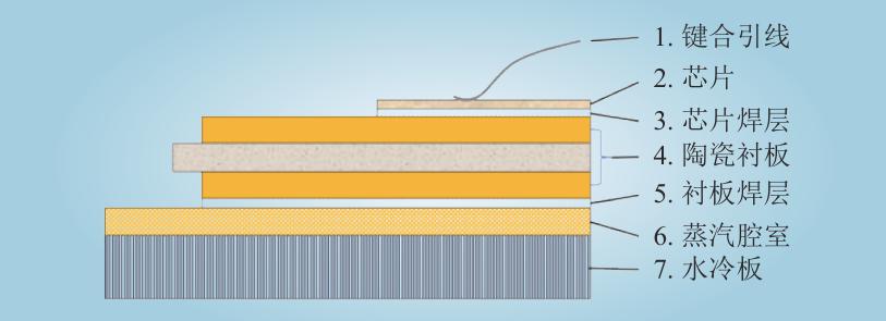
FIG. 9 IGBT module of substrate integrated phase change cooling structure
FIG. 10 IGBT module sample with integrated phase change cooling structure
Other thermal designs of module structure include substrate free structure, liner free structure such as die on leadframe (DOL), liner direct liquid cooling, liner substrate integrated design, integrated liquid circulation cooling channel, etc. The design goal is to simplify the module structure, reduce the bonding layer, remove the thermal interface material (TIM), achieve the reduction of thermal impedance, reduce Tj, increase the thermal stability and reliability.
In the module packaging process, advanced combination and interconnection technology can greatly improve the thermal stability of modules. The development of welding, sintering, and lead materials with higher thermal conductivity, or the use of large-area metal sheets instead of lead bonding technologies, such as direct lead bonding (DLB), can increase the flow and thermal conductivity, achieve uniform temperature distribution, and reduce excessive hot spots. ultrasonic bonding technique is used to connect terminal. The bonding layer between terminal and lining can be removed. The thermal mechanical stress can be greatly reduced and thermal stability can be enhanced.
2.3 Comparison of thermal resistance of different packaging structures
Test end-coolant thermal resistance (Rth j-f) for IGBT modules with different heat dissipation structures, as shown in Figure 11. Among the above three structures, DSC module has the highest heat dissipation efficiency and the lowest thermal resistance, which is the development trend of the next generation of high power density IGBT module. The experimental results verify that the heat dissipation efficiency of PCC structure is about 15% higher than that of DLC structure, which has a good application prospect in a certain extent and range. However, in the future period, due to the advantages of simple manufacturing process and application, DLC module will still be the mainstream products in the application fields of high performance and high reliability IGBT module, such as electric vehicles.
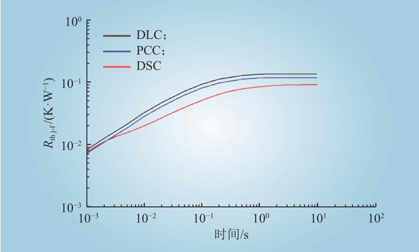
FIG. 11 Comparison of thermal resistance of IGBT modules with different heat dissipation structures
2.4 Thermal design of crimped IGBT module
The crimped IGBT (press pack IGBT) module is an ideal switching device for UHV flexible DC transmission system, and its full control and turn-off capability is the most critical requirement of voltage source converter. Currently, newly built UHV DC power transmission projects have entered the stage of IGBT module replacing high-power thyristors. For example, Zhangbei and Wudongde engineering, which have recently completed system tests, have adopted PPI module in part and in whole respectively, achieving the world's highest voltage level and the largest transmission capacity of flexible DC power transmission capability.
The packaging concept and structure of PPI module are derived from high-power thyristors. Large-area power terminals contact the front and back of multiple chips through pressure to interconnect the chips and form a parallel connection, thus improving the power capability. By design, the crimped packaging structure can achieve the goals of double-sided heat dissipation, failure and short circuit, which are the key requirements of HVDC transmission systems that need to achieve high voltage by connecting multiple power components in series. The non-plane interconnection structure of traditional welded IGBT module is inferior to PPI module in power capacity, heat dissipation, short circuit failure, reliability and other aspects.
FIG. 12 shows the basic structural unit and module structure profile of the CRRC era PPI module product. The basic unit is composed of chip, metal spacer, gate connecting pin and insulation frame. Through module-level packaging, multiple basic units are packaged in parallel in the module. The main components include ceramic shell, tube cover, tube seat, gate loop PCB and so on. Therefore, the thermal design of PPI module includes two aspects: basic unit level and module level.
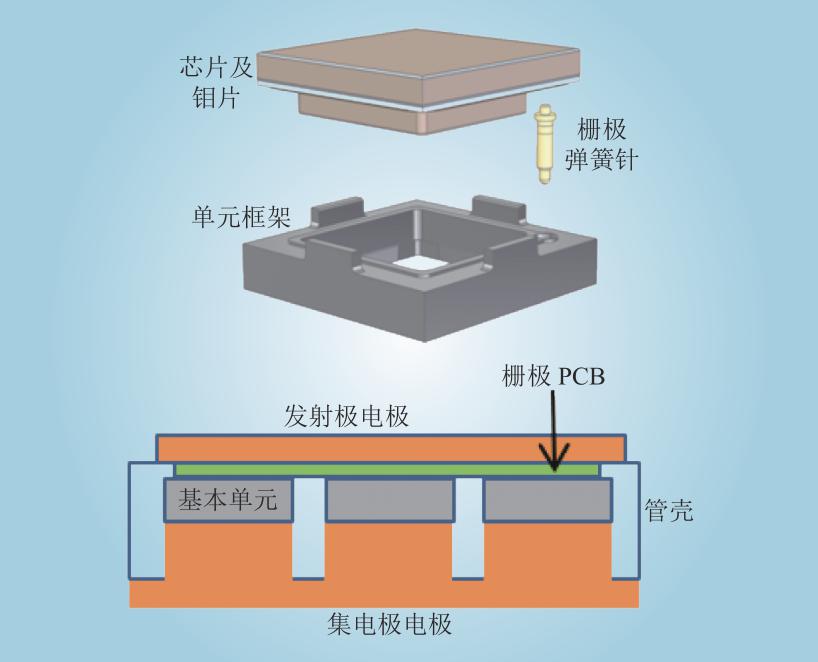
FIG. 12 Basic structural unit and overall structural profile of PPI module
According to the materials, dimensions, processes, application conditions and other information used in the PPI module, an accurate thermal simulation model can be established. These information can be represented in the thermal model in a reasonable way, and the temperature field distribution shown in Figure 13 can be output for the thermal management design and optimization of the PPI module. Figure 14 shows the transient thermal impedance curve of PPI module under different pressures. With the increase of press mounting force, the contact thermal resistance of the device decreases, the overall thermal resistance decreases, and the change of thermal resistance is also decreasing. According to its change rule, the range of press mounting force can be calibrated.
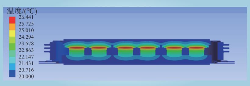
FIG. 13 Temperature distribution nephogram of PPI module under application conditions
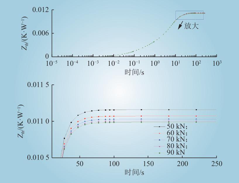
Fig. 14 Transient thermal impedance curve of PPI module under different pressures
3 Conclusion
The thermal performance and thermal stability of IGBT modules are important aspects of module design, characterization and application evaluation. Fast and efficient cooling of the chip is the key to packaging and application design. It will greatly improve the performance of IGBT modules, reduce the chip junction temperature and power loss, and thus improve stability and reliability. Especially with the increase of power density of IGBT modules, the harsh application environment, the improvement of reliability and life requirements, the thermal design and thermal management technology of IGBT modules is the most important link in the design and application of new products.
This paper mainly summarizes the thermal behavior and thermal design technology of traditional IGBT modules, as well as the thermal design of crimping IGBT modules for flexible DC transmission grid applications. Based on the thermal impedance network model of IGBT module, the thermal design and thermal management scheme of IGBT module are discussed from the aspects of packaging materials, structure and process technology.

